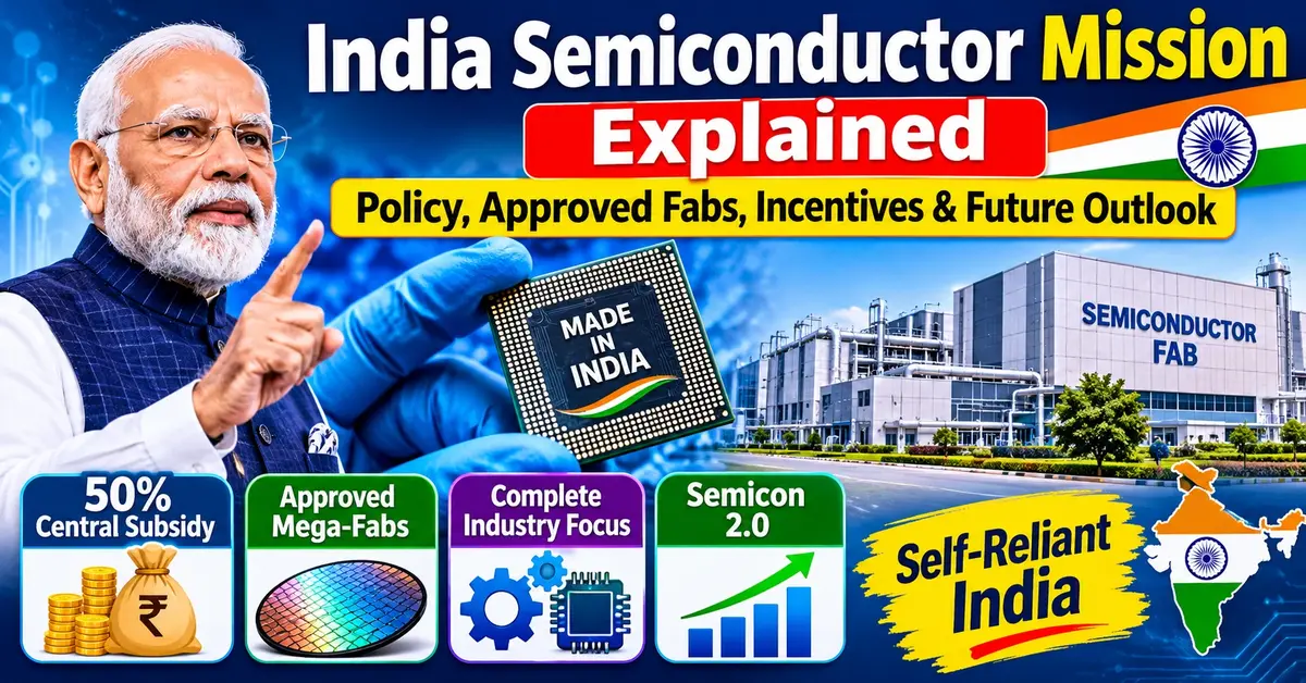
The Central Government launched the India Semiconductor Mission (ISM) as its core initiative to position India as a worldwide hub for semiconductor manufacturing. Launched in December 2021 under the Ministry of Electronics and Information Technology (MeitY), it started with a total budget of ₹76,000 crore (about $10 billion).
The mission runs as an independent business division inside the Digital India Corporation. Its goal is to set up a lasting local manufacturing base for semiconductors (microchips) and display panels.
To attract global companies, the policy offers a uniform 50% central subsidy on project costs. This applies to silicon wafer fabs (chip-making factories), packaging units, and compound semiconductor plants. State governments provide extra subsidies to make India a major global electronics manufacturing hub.
Key Takeaways
- Strong Financial Support: The Central Government pays 50% of the project setup cost (capital expenditure). It releases funds on an equal footing (pari-passu, meaning alongside the company’s own spending). Host states offer another 20% to 25% in top-up subsidies.
- Approved Mega-Fabs: Commercial projects worth over ₹1.6 lakh crore have already been approved. Key projects include Tata Electronics’ ₹91,000-crore wafer fab in Dholera, Gujarat, and Micron Technology’s ₹22,500-crore memory packaging plant in Sanand, Gujarat.
- Complete Industry Focus: The mission supports every stage of chip making. This includes front-end wafer fabrication, back-end packaging and testing (ATMP/OSAT), compound semiconductors, and design incentives for local startups.
- Focus on Mature Nodes: Initial factories will produce mature nodes (such as 28nm, 40nm, 55nm, and 91nm–110nm). These standard chips power 70% of global cars, power systems, factory machines, and telecom equipment.
- Scaling Up to Semicon 2.0: The government broadened the initiative by launching Semicon 2.0.This new phase supports chip-making machines, specialty gases, raw materials, workforce training, and the India Semiconductor Research Centre (ISRC).
What Is the India Semiconductor Mission (ISM)?
For decades, India was known for its chip design talent. Top global firms like Intel, Qualcomm, Texas Instruments, and Nvidia set up large design centers here.
However, India did not have a single commercial silicon wafer fabrication plant (called a “fab”). A fab is a specialized factory where raw silicon discs are turned into microchips. As a result, every chip used in Indian-assembled smartphones, cars, or defense systems had to be imported.
To solve this problem, the Union Cabinet approved the semiconductor program on 15 December 2021. The government created the India Semiconductor Mission (ISM) as a dedicated agency run by industry technocrats.
ISM acts as a single-window help desk for global chipmakers. It evaluates project proposals, approves financial aid, helps state governments arrange land and utilities, and tracks construction milestones.
Why India Needs a Domestic Semiconductor Policy
India’s push to manufacture chips locally rests on three critical reasons:
1. Protecting Against Supply Chain Disruptions
The global chip shortage during 2020–2022 showed how risky it is to rely on a few countries. Advanced microchip manufacturing is heavily concentrated in Taiwan, South Korea, and China. When global supply chains broke, Indian carmakers lost significant production. In many cases, assembly lines stopped because of a shortage of basic microcontroller chips that cost under ₹100 each.
2. Supporting Rapidly Growing Electronics Manufacturing
India’s electronics production has grown quickly under the Production Linked Incentive (PLI) schemes for smartphones and IT hardware. According to NITI Aayog projections, India’s domestic semiconductor market will cross $100 billion (about ₹8.3 lakh crore) by 2030. If India continues to import all these chips, its import bill could rival its crude oil import bill.
3. National Security and Defense Independence
Modern defense equipment requires trusted microchips. These include radar systems, secure radios, missile guidance controls, and satellite avionics. Relying on foreign supply chains creates risks of electronic spying, hardware bugs, and sudden supply cut-offs during geopolitical conflicts.
The Four Core Incentive Schemes Under ISM
In September 2022, the Central Government simplified the policy. It made the central financial subsidy a uniform 50% on an equal footing (pari-passu) basis across all manufacturing categories:
| Scheme Component | Target Facility | Central Government Financial Support | Key Eligibility Criteria |
|---|---|---|---|
| Modified Scheme for Silicon Fabs | Silicon CMOS Wafer Fabrication | 50% of Capital Expenditure (Project Cost) | Minimum 300mm wafer size, mature nodes (28nm to 110nm), established technology partner |
| Modified Scheme for Display Fabs | TFT LCD / AMOLED Display Fabrication | 50% of Capital Expenditure | Generation 6 or higher glass substrate production for screens |
| Modified Scheme for Compound & ATMP/OSAT | Compound Fabs (SiC/GaN) and Assembly/Test Units | 50% of Capital Expenditure | Minimum investment threshold: ₹100 crore for Compound Fabs; ₹500 crore for OSAT/ATMP units |
| Design Linked Incentive (DLI) Scheme | Fabless Chip Design Startups & MSMEs | Up to 50% of eligible design costs (capped at ₹15 crore per company) | Indian-owned and controlled companies building indigenous chip designs/IP |
Besides direct cash subsidies, the Design Linked Incentive (DLI) scheme supports Indian startups. Through the ChipIN Centre at C-DAC, engineering students and local design startups get cloud access to high-end Electronic Design Automation (EDA) software. These tools, from global leaders like Synopsys, Cadence, and Siemens, normally cost crores of rupees, so free access helps startups design chips without massive upfront capital.
Approved Semiconductor Plants in India
Under the first phase of ISM, the Union Cabinet approved multiple multi-crore facilities across India:
INDIA SEMICONDUCTOR PROJECTS: STATE-WISE INVESTMENTS
Gujarat: Dholera & Sanand
Assam: Jagiroad / Morigaon
Uttar Pradesh: Jewar
Odisha: Bhubaneswar
1. Tata Electronics & PSMC (Dholera, Gujarat)

- Facility Type: Commercial Silicon CMOS Wafer Fabrication Foundry
- Estimated Capital Outlay: Roughly ₹91,000 crore
- Strategic Collaborator: Powerchip Semiconductor Manufacturing Corp (PSMC), Taiwan
- Production Nodes: 28nm, 40nm, 55nm, 91nm, and 110nm on 300mm (12-inch) substrates
- Output Potential: Up to 50,000 wafer starts per month (WSPM)
- Applications: Power regulation circuits, microcontrollers, display driver ICs, and automotive semiconductors destined for electric vehicles, home electronics, and telecom infrastructure.
2. Micron Technology ATMP (Sanand, Gujarat)

- Facility Type: Assembly, Testing, Marking, and Packaging (ATMP)
- Estimated Capital Outlay: Approximately $2.75 billion (roughly ₹22,500 crore, backed by $825 million in corporate equity)
- Core Output: Packaging and validation services for dynamic random-access memory (DRAM) and NAND flash storage solutions.
- Target Markets: International supply chains supporting enterprise computing devices, flagship mobile phones, and hyperscale data centers.
3. Tata Semiconductor Assembly and Test (Jagiroad, Morigaon, Assam)

- Plant Category: Outsourced Semiconductor Assembly and Test (OSAT)
- Estimated Capital Outlay: Around ₹27,000 crore
- Processing Capacity: Up to 4.8 crore (48 million) finished components per day
- Economic Significance: Stands as the largest private-sector industrial venture across Northeast India, packaging microchips for consumer hardware, automotive systems, and industrial automation.
4. CG Power, in partnership with Renesas Electronics and Stars Microelectronics, located in Sanand, Gujarat.

- Facility Type: OSAT Facility
- Estimated Capital Outlay: Near ₹7,600 crore
- Project Partners: CG Power from the Murugappa Group, Japan’s Renesas Electronics, and Thailand-based Stars Microelectronics.
- Primary End-Uses: Automotive sensing components, power management electronics, and industrial motor control modules.
5. Kaynes Semicon (Sanand, Gujarat)

- Facility Type: Advanced Packaging and OSAT Center
- Estimated Capital Outlay: Approximately ₹3,300 crore
- Output Volume: 60 lakh (6 million) packaged ICs daily for industrial automation, aerospace avionics, and vehicle electronics.
Front-End Fabs vs. Back-End OSAT Facilities
Industry terminology often conflates front-end fabrication with back-end packaging. India’s strategic roadmap encompasses both stages of the semiconductor production lifecycle:
01. Silicon Ingot & Slicing
High-purity silicon ingots are sliced into thin silicon wafers.
02. Front-End Fabrication (The Fab)
- Cleanroom standard: ISO Class 1 (ultra-clean environment)
- Core operations: Photolithography, ion implantation and chemical etching
- Representative site: Tata-PSMC Dholera Plant
03. Processed Silicon Wafer
Completed wafer containing multiple fabricated semiconductor chips (dies), ready for back-end processing.
04. Back-End Packaging & Testing (ATMP / OSAT)
- Dicing wafers into individual semiconductor dies.
- Wire bonding or flip-chip attachment to substrates.
- Protective epoxy molding and thermal/electrical testing.
- Representative sites: Micron Sanand, Tata Assam and CG Power.
05. Final Packaged Microchip
Finished and tested semiconductor chips, prepared for surface-mount soldering onto printed circuit boards (PCBs).
Front-End Fabrication (The Fab)
This represents the most capital-intensive and technologically demanding phase. Raw silicon discs undergo hundreds of light-printing and chemical transformations inside ultra-pure cleanrooms, etching billions of microscopic transistors onto every wafer.
Back-End OSAT / ATMP Operations
An OSAT or ATMP facility takes completed wafers, slices them into individual dies, attaches fine copper or gold interconnect wires to package pins, seals the assembly in protective molding compound, and screens parts under heavy thermal and electrical stress.
Establishing OSAT facilities initially provides India with rapid milestones. These plants can immediately service domestic circuit board manufacturers for smartphones and automobiles, whereas front-end silicon fabs require a 3-to-4-year gestation timeline.
Rationale Behind Targeting Mature Nodes (28nm to 110nm)
Critics occasionally question why India is not initially constructing leading-edge 2nm or 3nm fabs comparable to TSMC’s Taiwan plants. The national strategy prioritizes mature nodes due to sound economic and market realities:
- Broad Domestic Demand: Ultra-small geometries (sub-7nm) target high-end smartphones and artificial intelligence accelerators. Conversely, automobiles, industrial machinery, smart meters, and defense electronics rely primarily on robust 28nm to 110nm microcontrollers and power management ICs.
- Reduced Financial and Technical Risk: A cutting-edge 3nm plant demands expenditures exceeding $20 billion alongside restricted Extreme Ultraviolet (EUV) lithography systems. Conversely, a mature 28nm fab requires $5 billion to $10 billion, utilizes dependable equipment, and achieves commercial manufacturing yields much faster.
- Immediate Local Integration: Indian manufacturing ecosystems can immediately consume mature-node microchips within electric vehicles, smart energy grids, digital payment soundboxes, and 5G base stations.
Regional Policies and Infrastructure Support
While the Central Government funds half of approved project expenses, individual states compete by offering supplementary financial grants, discounted utilities, and dedicated industrial land:
- Gujarat: Enacted the Dedicated Semiconductor Policy (2022–2027), providing an additional 20% state subsidy—bringing cumulative public funding to 70%—alongside subsidized land allocations within the Dholera Special Investment Region (SIR) and Sanand, reliable water utility pipelines, and reduced electricity tariffs.
- Assam: Formulated the Assam Semiconductor Policy, supplying expansive industrial land tracts in Jagiroad alongside steady, clean power infrastructure for Tata’s packaging venture.
- Uttar Pradesh: Grants 25% state capital assistance on top of federal incentives, successfully attracting the HCL-Foxconn partnership near the upcoming Jewar International Airport.
- Odisha: Concentrates efforts on compound semiconductor manufacturing (specifically Silicon Carbide), provisioning dedicated water corridors, power subsidies, and research grants in Bhubaneswar.
The Next Evolution: Semicon 2.0 (ISM 2.0)
Following the widespread allocation of the initial ₹76,000-crore budget across sanctioned projects, the Union Cabinet greenlit Semicon 2.0 backed by an expanded financial outlay of ₹1,27,500 crore.
Sustainable chip manufacturing relies on complete localized supply chains. Semicon 2.0 centers on six strategic pillars:
- Equipment and Tooling: Fiscal incentives encouraging domestic and international entities to manufacture lithography machinery, etching systems, and testing hardware locally.
- Specialty Gases and Chemicals: Domestic synthesis of high-purity chemicals (such as hydrofluoric acid) and industrial gases (including silane and argon).
- Advanced Packaging and Fabs: Financial backing for next-generation 3D packaging technologies and additional silicon wafer fabs.
- Research and Development: Establishing the India Semiconductor Research Centre (ISRC), structured along the lines of Belgium’s IMEC and Taiwan’s ITRI, to collaborate with premier Indian Institutes of Technology (IITs) on indigenous IP.
- Talent Pipeline Development: Modernized academic curriculums deployed across 300+ institutions to train 85,000 skilled semiconductor professionals over five years in cleanroom operations and chip architecture.
- Compound Semiconductors: Fostering native manufacturing capabilities for Gallium Nitride (GaN) and Silicon Carbide (SiC) to support electric vehicle powertrains and solar inverter systems.
Primary Hurdles Confronting the National Mission
Establishing a commercial microelectronics manufacturing ecosystem from the ground up introduces significant operational hurdles:
- Intense Utility Demands: A single silicon fabrication facility requires between 10 million and 15 million liters of ultrapure water daily. Furthermore, operations demand absolute electrical continuity; even a millisecond voltage drop can irreparably ruin an entire production run of silicon wafers.
- Heavy Import Dependence: Fabs require hundreds of special chemicals and gases. Until Indian chemical makers achieve extreme purity levels, fabs will continue to rely on imports from Japan, Europe, and the US.
- Cleanroom Talent Shortage: India has thousands of talented chip design engineers, but very few technicians trained to work inside high-tech cleanrooms or run complex etching machines. Bridging this gap will require training and global partnerships.
- Long Construction Timelines: Fabs typically take 3 to 4 years to build, calibrate, and get certified by commercial buyers. Keeping policies and incentives stable across election cycles is critical for success.
Frequently Asked Questions
What is the main objective of the India Semiconductor Mission?
The India Semiconductor Mission (ISM) was set up to build a self-reliant chip design, manufacturing, and packaging ecosystem in India. Its goal is to reduce import dependence, protect local car and electronics factories from global shortages, and turn India into a trusted global supplier of microchips.
How much subsidy does the Indian government provide for semiconductor plants?
The Central Government provides a uniform 50% subsidy on the capital cost of approved silicon wafer fabs, display fabs, compound semiconductor plants, and OSAT/ATMP units on an equal footing (pari-passu) basis. State governments provide an additional 20% to 25% subsidy, covering up to 70% to 75% of the total project cost.
Where is the country’s inaugural commercial chip fabrication facility situated?
The establishment of India’s inaugural commercial silicon wafer manufacturing facility is currently progressing in Dholera, Gujarat. It is being built by Tata Electronics in partnership with Taiwan’s Powerchip Semiconductor Manufacturing Corporation (PSMC) with an investment of about ₹91,000 crore.
What is the difference between a semiconductor fab and an ATMP/OSAT unit?
A semiconductor fab (front-end) makes microchips from scratch by printing electrical circuits and transistors onto raw silicon discs inside ultra-clean rooms. An ATMP/OSAT plant (back-end) takes those completed wafers, cuts them into individual chips, attaches protective casings and connecting wires, and tests them before they are placed onto device circuit boards.
What process technology nodes will be manufactured in India?
India’s initial manufacturing plants will focus on mature process nodes between 28nm, 40nm, 55nm, and 91nm–110nm. These nodes are widely used in car engines, electric vehicles, industrial machines, smart meters, home appliances, and telecom equipment.
Final Takeaway
The India Semiconductor Mission is one of the most ambitious industrial policy efforts in modern Indian history. By replacing fragmented schemes with a simple 50% central cost-sharing model, India has attracted major investments from leading domestic and global companies.
Building a full semiconductor supply chain will take years of steady government funding, reliable power and water infrastructure, and extensive workforce training. However, with multi-crore fabs and packaging units now under construction in Gujarat and Assam, India is moving from being just a consumer of electronics to an active player in global chip manufacturing.
Read This Also:
What Is Prompt Engineering? 5 Rules for Writing Better AI Prompts
1 thought on “India Semiconductor Mission: Policy, Approved Fabs & 5 Major Projects”